satti@subassociates.com
+1(408) 262-4100
Our Management Team
Hafeez Raja, CTO & Founder
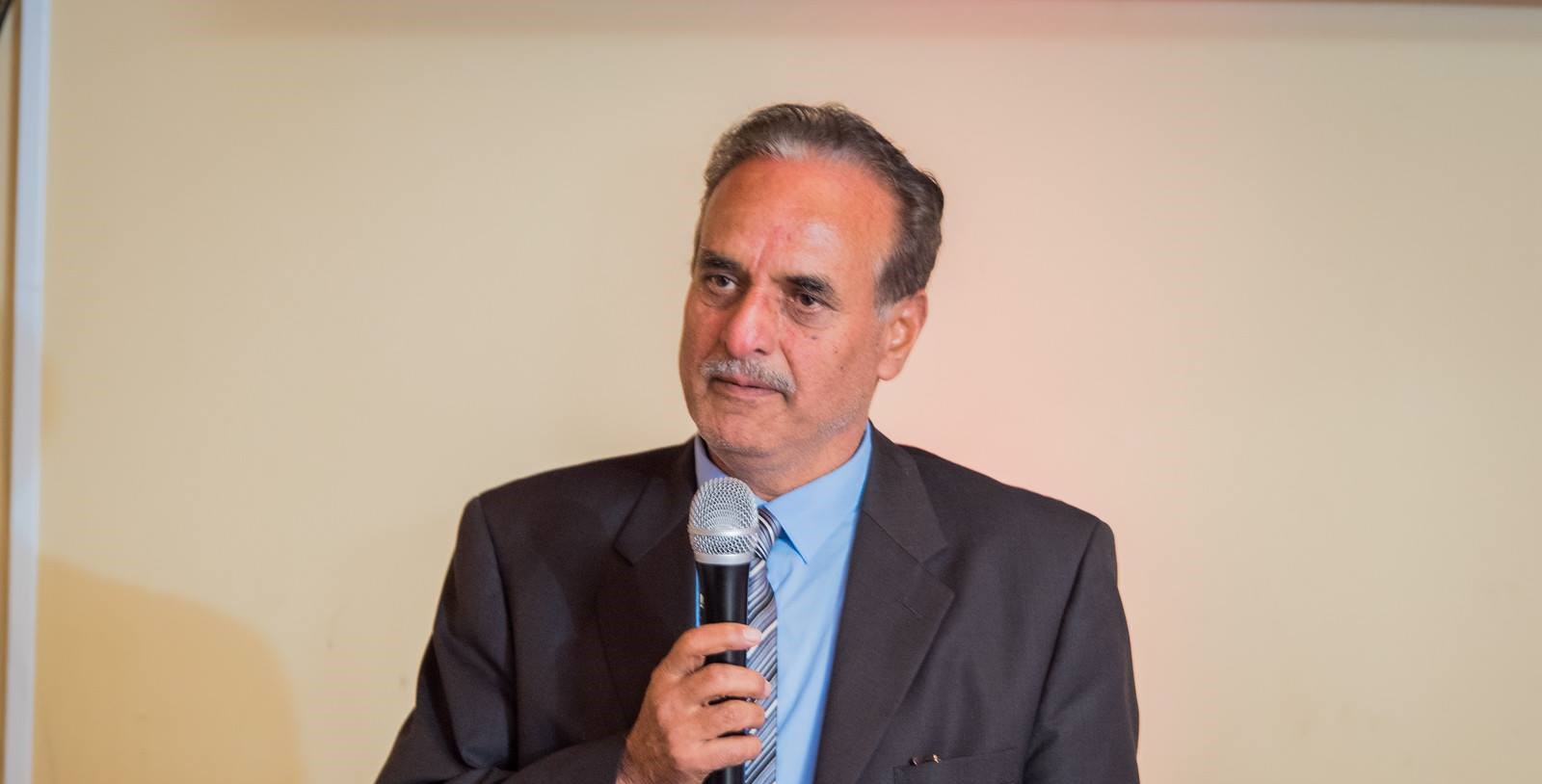
The dynamic initiative team led by Hafeez Raja, a proven High Tech executive with over 25 Years of Silicon Valley business and technology knowledge. He has a Track Record of success as an Executive at both large multi-national technology firms & Silicon Valley startups. He has led Multi-national teams, both large and small through difficult Turn-Arounds, and succeeded in very challenging business environments. He excels at simultaneously balancing Business, Technology, logistics, professional staffing and financial issues.
His support for his clients in achieving the customer's business goals to surpass current microelectronics, fiber optics, semiconductor, wireless communications, LEDs, LDs, clean technology, solar energy, and nanotechnology industry standards. The comprehensive training and “unified front” philosophy enables us to deliver the level and quality of our service regardless of the customer’s approach.
He has held several high-level technical, business development, marketing and managerial positions including CTO, VP Business Development, Customer Engagement Leader for Western region, Asia and Europe, Principal Technologist, program manager, Principal Applications engineer, Executive Director Sales & Marketing, Program Director, Adjunct faculty member and Research Engineer. He has worked with culturally diverse people and demonstrated strengths in strategic planning and organization. In addition to a Ph. D course work in optics, Hafeez Raja holds a Masters in Electrical Engineering and Masters in Engineering Management from Florida Institute of Technology; holds Masters in Nuclear Physics from Government College University, Lahore and M.Phil in solid state physics from University of the Punjab, Lahore. His accomplished career includes: characterization & optimization of RTP for micro-contamination & Silicide formation in semiconductor processing and equipment. His thesis project focused on Radiation Hardening, investigating the impact of Cosmic rays, Gamma rays, Beta rays, and X-rays on devices in space. His excellent research work in designing and building first multi-target chamber used to study nuclear energy levels of light nuclei with (proton, gamma) reaction before the cluster tool concept was a major breakthrough in research arena. In addition, he has extensive work experience on photoconductivity of the refractory metals in UHV systems. His significant contribution to the semiconductor processing clustered tool is distinctive.
Seminars: Hafeez Raja has conducted a variety of seminars and training courses including Stress Management, Total Quality Management, Customer Relationship Manager which includes conflict resolution, ethics, effective communication, harassment, and dialogue opening. Additonal seminars entail Quality Service Skills, Employment Uniqueness, Instructional Techniques, Future Technology Market Trend, Semiconductor Processing, OEM requirements and III-V Market.
Areas of Expertise Include:
- Resolving Complex Issues at Corporate, Divisional and Team levels.
- Strategic Planning for Business, Technology and Intellectual Property.
- Global business management, Sales, marketing & product development.
- Business Results & processes for both startups and large corporations.
- Organizational Development, Team structure and Driving Execution.
Projects
Hafeez Raja is a goal-oriented strategic professional with a critical thinking approach utilizing his engineering management and technical post-graduate degrees and over twenty years of experience offering services as a Business Development Executive. He has managed an exhaustive database of over 6,000 professionals and 2,500 industrial contacts. His projects over the time include:
Customer Engagement Leader, Western Region, Asia & Europe, Taiyo Nippon Sanso Corp, CA. 99– 2001:
- Monitored competitor’s business practices, strategies, and tactics
- Served as the management liaison to key customers, partners, and national accounts
- Worked with sales to identify opportunities & helped develop winning sales strategies
- Developed and managed training program for the OEM customers and sales/marketing force
- Reviewed employee professional development and performance quarterly/annually in the region
- Responsible for providing recruiting, training, motivation, and leadership for the regional salesforce
- Played an instrumental role in leading the microelectronic industry with technology engineering services
- Led Compound Semiconductor Initiative (CSI) Team for the customer’s Critical-To-Quality (CTQs) issues in the Western region, Asia (Pacific Rim), and European territory
Principal Application Engineer, Emerson Co, Semi Group, Fremont, CA
- Supported system & process integration regarding Brooks products & explored new applications
- Provided technical information and briefed the sales team for customer meetings and presentations
- Managed to reduce cost and enhance productivity by 40% with the concept of training as an investment
- Responsible for bringing semiconductor industrial future needs and customer feedback to the sales force, engineering, and manufacturing while directing future product requirements
Sr. Process Application Engineer, Gasonics (LAM Research), Semi Team, San Jose, CA
- Protected product line of plasma etch/ash equipment, Intel Operating Unit (IOU)
- Trained customers and field service engineers to minimize service request load
- Enhanced process at customer sites and characterization of new product
- Interfaced with the customer during demos, written demo reports, and lab-sustaining work
- Coordinated sales, marketing, engineering, and service department
Research Engineer, Intersil (Harris Semiconductor, Process Technology Group) Palm Bay, FL
- Characterized thermal performance of Rapid Thermal Processing machine (RTP)
- Developed new techniques for analyzing the thermal profile of wafers during processing
- Worked with dielectric reflow (BPSG) parameters and tungsten silicide annealing cycles
- Monitored the silicide formation and changes in the sheet and contact resistance of Wsi2
- Optimized RTP applications for precise temperature control in ULSI product development
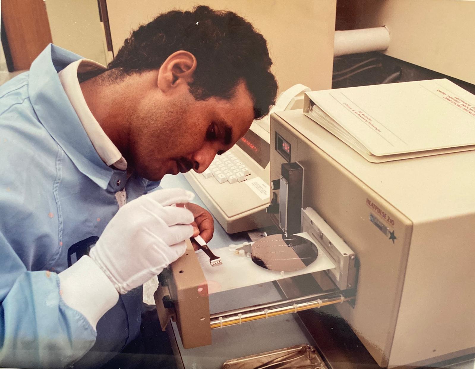
Hafeez Raja conducts research on characterizing thermal performance on Rapid Thermal Processing (RTP) standalone machine
He then moved on to become VP, Sales & Marketing, Hi-Tech Laser, Santa Clara, CA from 2001 - 2003
- Led the definition, positioning, pricing, and promotion of the product
- Responsible for recruiting, training, motivating, and mentoring business unit
- Developed a marketing strategy and built a sales and marketing organization
- Utilized all sales reporting, management tools & systems to achieve sales objectives
- Effectively maintained and conformed to regional sales budget and profitability goals
- Interacted with the C-level and navigated across multiple levels of complex organizations
- Coordinated with the analyst community and industry experts to identify emerging issues
- Performed competitive analysis, Mentored the development & execution of marketing strategies
Western Region Customer Services, Business Development, & Technical Consultant from 2003 - 2010 where his work entailed
Executive staffing, training, advisory, and organizational development was the core purpose of working with the following companies in North America: Kineto Wireless; Ortiva Wireless; Silver Peak Systems; Magnum Semiconductor; Applied Energy Systems, Inc.; Cavium; Allot Systems; Headway Technologies; Maxim Semiconductor (Dallas Semiconductor); Sonicwall; Research in Motion Limited (Blackberry Limited); Thermosensors; US Desal; China Cache; Dust Networks; Neterion (Exar); Teros, Inc. (Citrix); Swagelok; Applied Materials; NASA Ames; Eco-Snow Systems (The Linde Group); Xyratex; Fluxion; Northern California Chapter American Vacuum Society (NCCAVS)
Hafeez Raja's working experience in companies based in the USA extends far beyond geographical boundaries, encompassing a diverse spectrum of industries, cultures, and professional environments as detailed below.
- Micron, Boise, DELCO, ID; Silane (siH4) processing clean room issues on the OEM tools.
- SEH, Vancouver, Oregon, resolving wafer processing contamination issues.
- Intel, Fab D1, Aloha, D2, Santa Clara qualifying 300mm tools resolving Quartz contaminations.
- Hitachi, Brisbane, San Francisco, OEM processing tool qualifications.
- AMD, Fab 25 in Austin, Texas, and Fab 30 in Dresden, Germany.
- HP in Texas Bulk Gas delivery system for batch-to-batch process consistency.
- Brooks Instrument, Working on Mass Flow controllers, Mass Flow meters, transducers, and Totalizers. Conducted thorough competitive product research for marketing purposes, which includes Unit, Tylon General, ports, and MKS tools.
- Designed toxic gases pipeline from POS to POU, using Arsine, Phosphine, Ammonia, H2So4, NF3, and all other semiconductor and compound semiconductor process gases.
- Designed, coordinated, led engineering group, and marketed Gas-Tunners that have the capacity of the equivalent of 450 cylinders for process consistency, repeatability, and reproducibility in foundries and Fabs worldwide.
- Consolidated service centers to reduce inventory, cost, and the headcounts efficiently.
- Worked on OEM tools from AMAT, LAM research, Hitachi, Novelus, Mattson Technology, EMCORE, TEL, Aixtron, NXP, and KLA-Tencore to qualify for etching, deposition, CMP, from crystal growth to polishing, doping, masking, etching, depositing, slicing, and pre-post cleaning processes. Resolved Quarts contamination long pending issues at INTEL, D1, class-1 fab.
- Working closely with gas companies like API, BOC, Matheson, NiponSanso, Scott Specialty, Linde, Air Liquide, etc.
- Worked closely with TSMC, UMC in Taiwan, and other chip manufacturing foundries, like SAMSUNG, HYNDAi, Seamens, OSRAM, Infineon, INTEL, AMD, etc.
- Worked with numerous LED manufacturers, like Lumiled, Gelcore, CREE, Nichia, Epistar, EPI, Lightwave, Nova Crystal, NovaLux, etc.
- Extensive work done on refractory metals, like Tungston, tantalum, Titanium, Molybdenum, Silicide formation for sheet resistance and contact resistance formation.
Advisory Committee
Members of the Advisory Committee:
Kambiz Farnaam, Ph.D
Dr. Kambiz Farnaam acquired his Masters and Ph.D from UC Berkeley in Nuclear Engineering in 1982. Worked for AMD, Thermawave, Novellus, and Applied Materials.
Mohamed Saleem, Ph.D
Dr. Mohamed Saleem is the CTO of Brook's Instrument. An active participant in the standards activities of gas-panel, corrosion, surface-analysis, stainless-steel task forces of SEMI, Saleem has published several papers in the field of materials science and engineering, and has presented many papers at major conferences. He received an M.S in Chemical Engineering from Tufts University in Medford, MA, and a Ph.D in Materials Science and Engineering from the University of Florida in Gainesville, FL.
Ashish Bhatnagar, Ph.D
Dr. Ashish Bhatnagar has over 14 years of experience in semiconductor processing technology, gas chemistry, and chemical synthesis. He is accredited with patents, awards, presentations, and publications. He received his Ph.D. in Chemical Engineering from the University of Minnesota. Dr. Bhatnagar is an Engineering Manager with a Fortune 500 company in the semiconductor field. He has successfully managed several programs in the area of Semiconductor fabrication process development and plasma processes.
Souvik Banerjee, Ph.D
Dr. Souvik Banerjee received his Ph.D from the University of Arkansas in Instrumental Sciences. Currently, he’s associated with a Fortune-Hundred company as a Director of Business Development. He worked for Novellus Inc. and Komag Inc.
Quick Links
© SUB Associates, LLC®. All Rights Reserved.